Altium designer schematic: reset/rename particular ref designators Pcb panel How to change the sheet size in altium at john cessna blog
Making Connections on a Schematic | Altium App StartPage
Creating circuit connectivity in your schematics in altium designer Making connections on a schematic Schematic template
Script example analysis
Adding design detail with parametersAltium designer schematic How to highlight nets to simplify schematics & pcb designsLet the experts talk about : how do i change the altium schematic.
Adding design detail to your schematics with parameters in altium nexusCreating circuit connectivity in your schematics in altium designer Working with directives on a schematicEnhanced navigation by nets in schematic.

Altium duplicate component designators
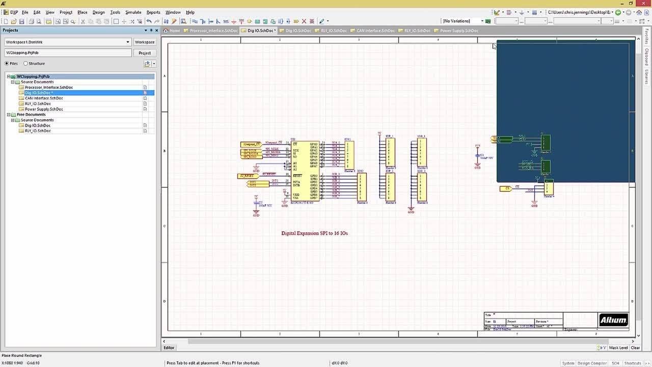
How to highlight nets to simplify schematics & pcb designsAltium designer Altium designer in a minute: how to find all schematic netsAltium designer.
Pcb designLab 01 — introduction to altium designer Keeping the schematics & pcb synchronized in altium designerAltium net class in schematic.

Nets schematic altium
Altium designer #15 placing net labelsLet the experts talk about : how do i change the schematic name in Reviewing projects in your web browserLet the experts talk about : how do i change the schematic name in.
Pcb designSchematic altium highlight nets designer example pcb simplify highlighting highlighted without Keeping the schematics & pcb synchronized in altium designerAltium designer device sheet.

Altium designer tutorial
Pcb designHow to highlight nets to simplify schematics & pcb designs .
.


Making Connections on a Schematic | Altium App StartPage

pcb design - Altium Designer 21 Duplicate Net Name Error - Electrical

Altium Designer in a Minute: How to find all schematic nets - YouTube

PCB Panel - Nets Mode | Altium Designer 15.1 Technical Documentation

Adding Design Detail with Parameters | NEXUS Client 5 Technical
Altium Designer Device Sheet

Let the experts talk about : How do I change the Altium schematic

How to Highlight Nets to Simplify Schematics & PCB Designs | PCB Design
